


Synthesis of Two-Dimensional Tungsten Trioxide (WO3) Nanostructure and Its Application in Photodetectors
-
摘要: 三氧化钨(WO3)是制造晶体管和光电探测器的理想材料,虽然在WO3纳米结构的生长方面已经完成了一些工作,但是制造足够长的理想型纳米线仍然是一个挑战。在众多的合成方法中,作者选择了化学气相沉积(CVD)方法合成WO3纳米线,并对其在光电传感器中的应用进行了研究。影响WO3纳米线成品率的主要因素是前体材料温度、基片位置、载气流速和生长持续时间。在合适的生长条件下生长的纳米线长度最长约为100 μm。这些WO3纳米线可用来制造高性能的光电探测器,WO3光电探测器具有灵敏度高、响应速度快、模块微型化等优良的器件性能,表明二维WO3纳米线在光电探测器的制造中具有很大的优势。Abstract: Tungsten oxide (WO3) is ideal for manufacturing transistors and photodetectors. Although some work has been done on growth of WO3 nanostructures, making ideal long enough nanowires is still a challenge. Among many synthesis methods, the author chose to use chemical vapor deposition (CVD) to synthesize WO3 nanowires and study their application to photoelectric sensors. The main factors affecting WO3 nanowires products are precursor material temperature, substrate position, carrier gas flow rate and growth duration time. The greatest length of nanowires grown under appropriate growth condition is approximately 100 μm. WO3 nanowires can be used for fabricating high-performance photodetectors. WO3 photodetector has excellent device performance including high sensitivity, fast response speed and module miniaturization, which indicate that two-dimensional WO3 nanowires have great advantages in the manufacture of photodetectors.
-
Key words:
- WO3 /
- Photodetector /
- Two-dimensional materials /
- Nanostructure
-
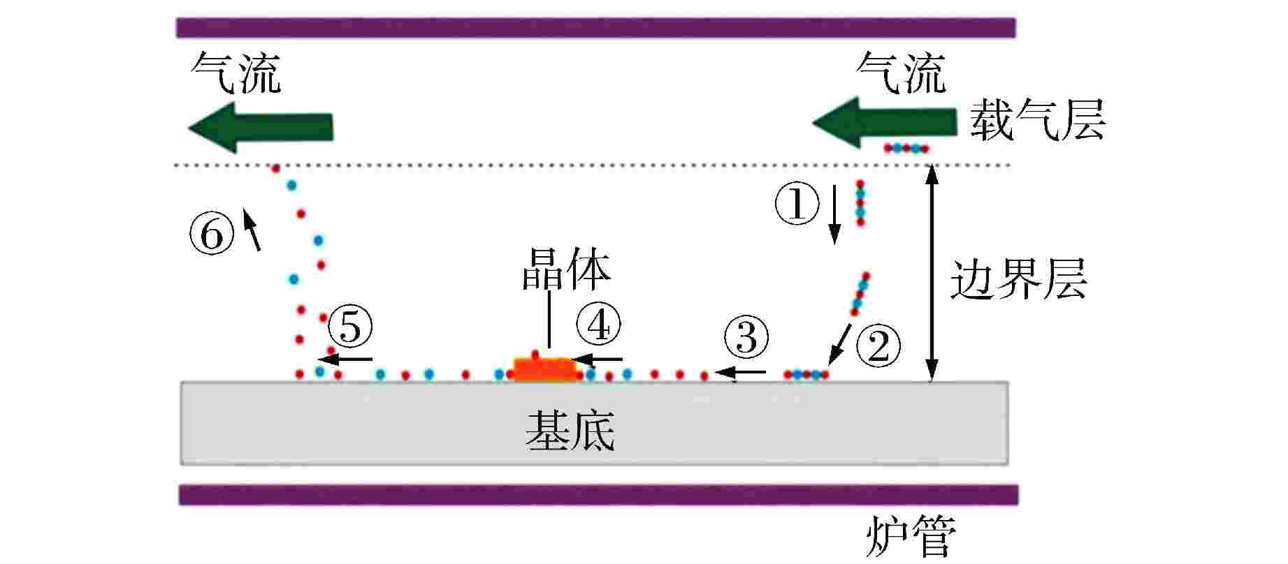
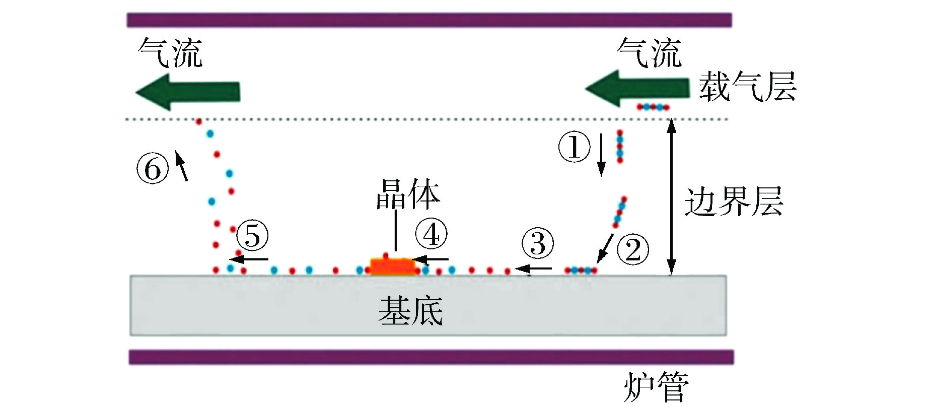
图 1 CVD过程中的生长机理示意图
蓝色点—W原子;红色点—O原子
Figure 1. Schematic Growth Mechanism during CVD Process
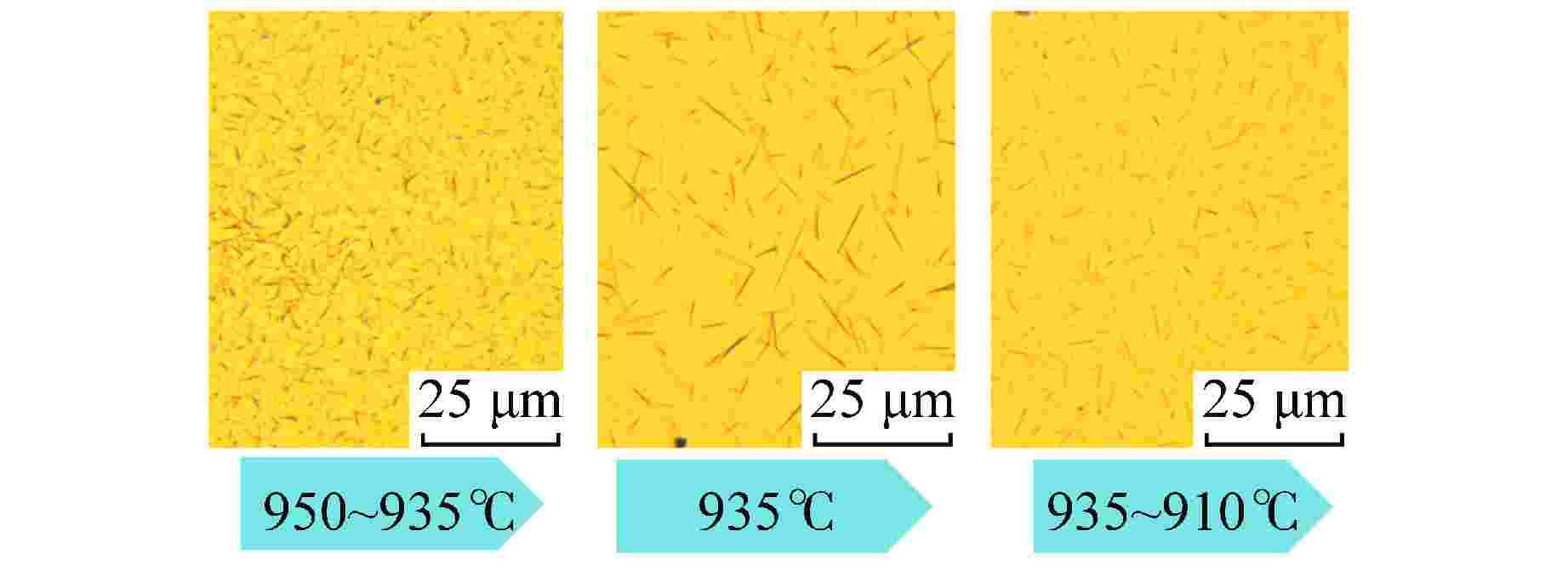
图 3 在不同前体材料温度下生长的WO3纳米线
Figure 3. WO3 Nanowires Grown at Different Precursor Material Temperatures
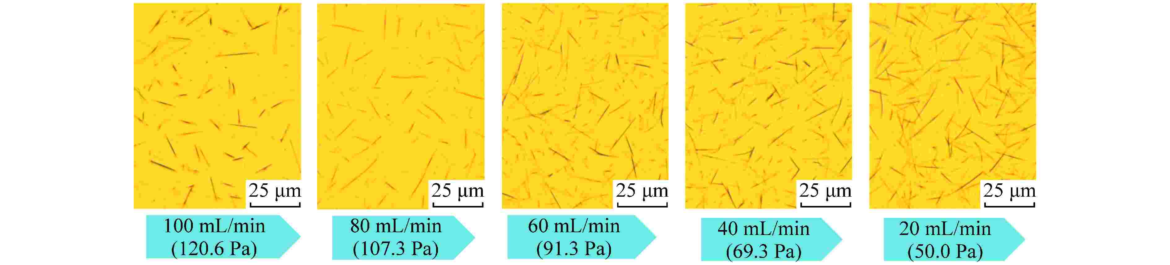
图 6 以不同载气流速生长的WO3纳米线
Figure 6. WO3 Nanowires Grown with Different Carrier Gas Flow Rate
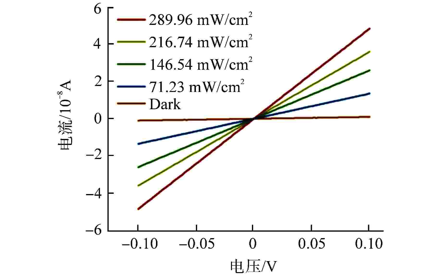
图 8 WO3单纳米线光电探测器的光响应行为
Figure 8. Photo-response Behaviour of WO3 Single Nanowire Photodetector
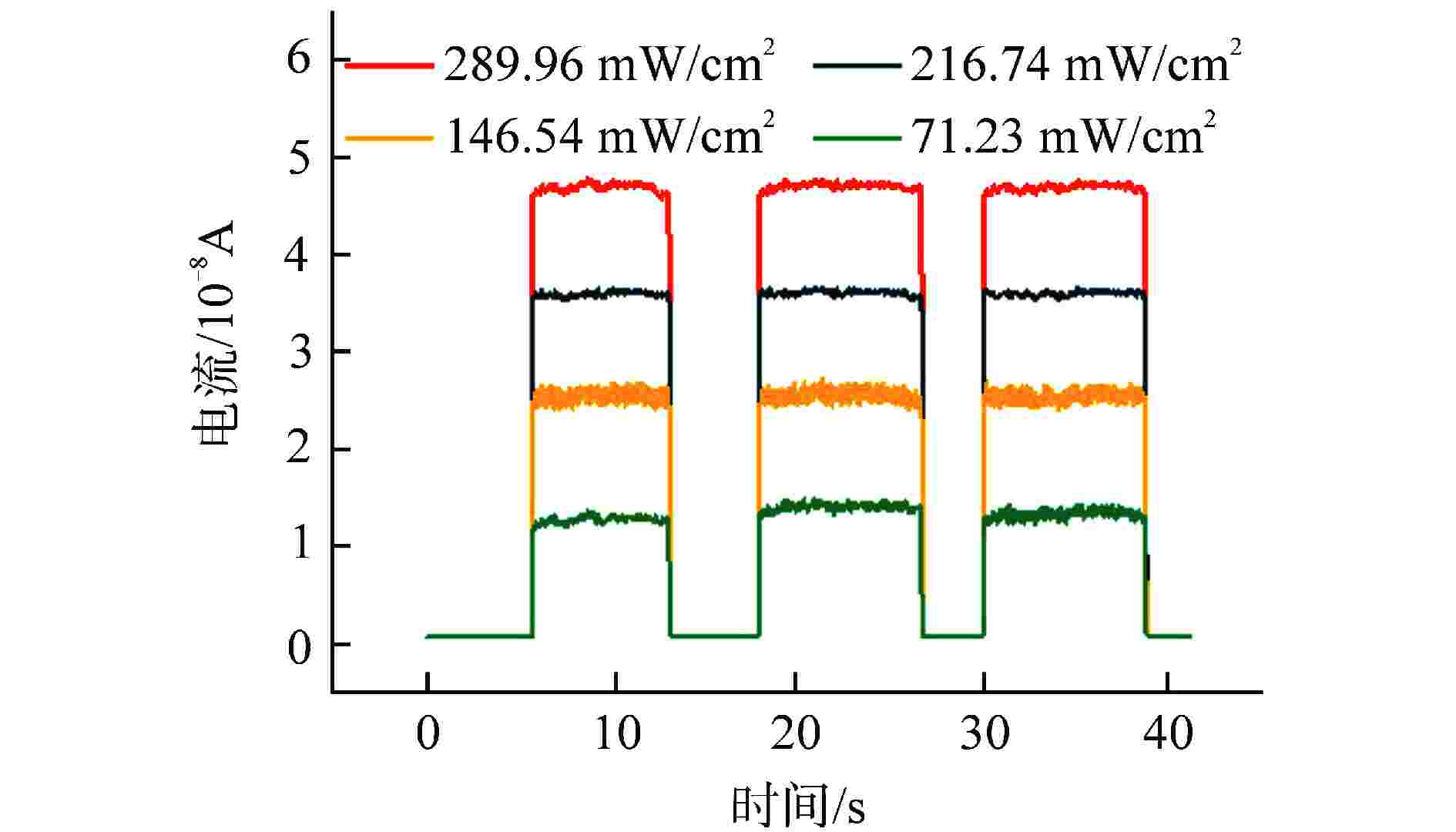
图 9 WO3单纳米线光电探测器在0.1 V偏压下的光开关行为
Figure 9. Photo-switching Behavior of WO3 Single Nanowire Photodetector under a Voltage Bias of 0.1 V
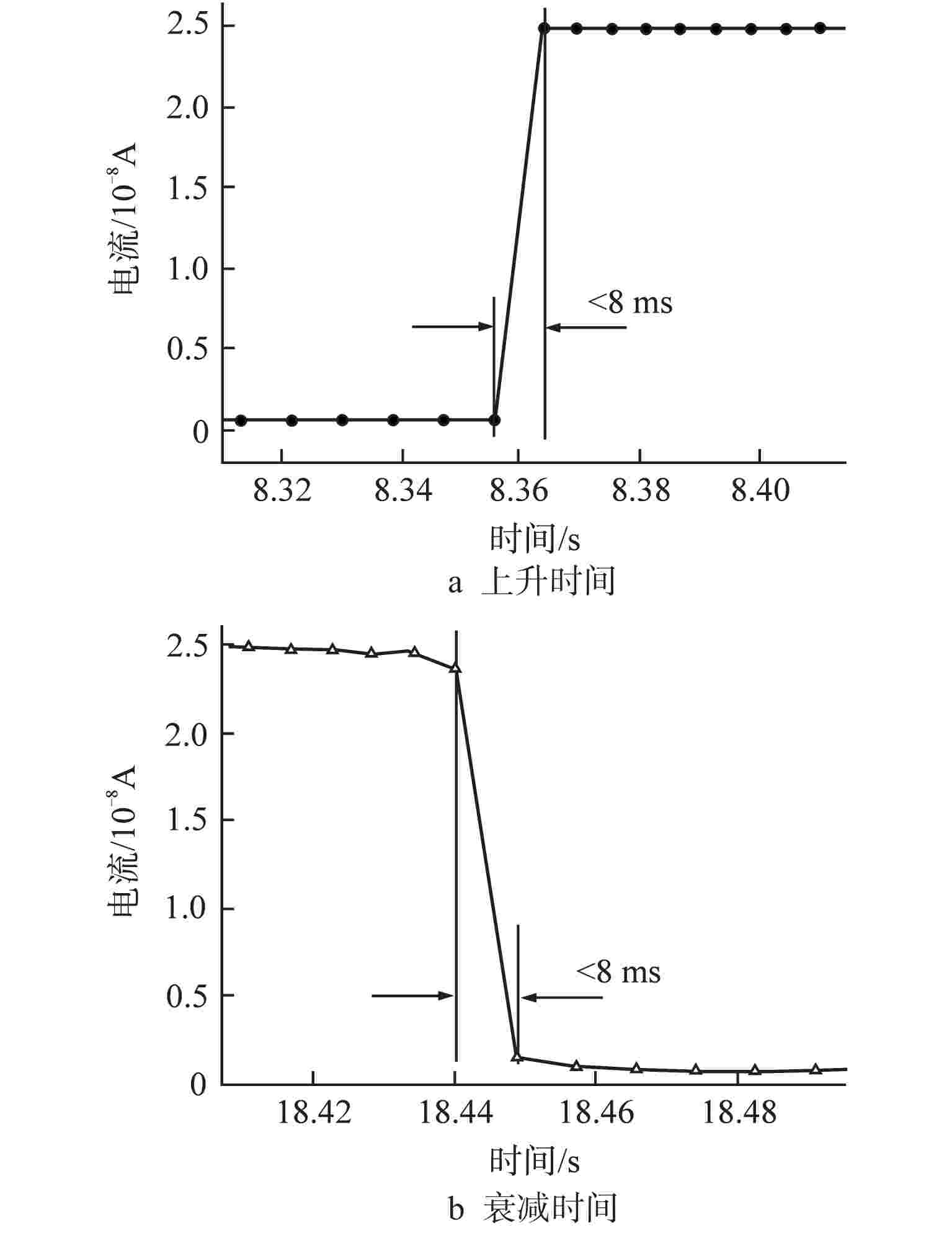
图 10 WO3纳米线光电探测器的上升时间和衰减时间
Figure 10. The Rising Time and Decay Time of the WO3 Nanowire Photodetector
表 1 基于纳米结构半导体的光电探测器的性能
Table 1. Performance of the Photodetector based on Nanostructured Semiconductor
材料名 响应度/
(A·W−1)光电
开关比特定
检测度/J响应
速度/msCdTe 6×10⁻⁴ 27 5.8×10⁹ 14.7 CdSe 100 1.7 — 24 PbS — <2 1.0×10¹¹ 300 Bi2Te3 5.5×10⁻² 1 5.9×10⁷ 1043 Bi2Se3 1×10⁻² 1.67 4.63×10⁸ 37 InSb 8.4×10⁴ — — 260 WO3 19 50 1.06×10¹¹ 8 “—”表示参考文献中无体现  下载: 导出CSV
-
[1] SZÉKELY I, KOVÁCS G, BAIA L, et al. Synthesis of shape-tailored WO3 Micro-/Nanocrystals and the photocatalytic activity of WO3/TiO2 composites[J]. Materials, 2016, 9(4): 258. doi: 10.3390/ma9040258 [2] WANG H, LIU J L, WU X X, et al. Ultra-long high quality catalyst-free WO3 nanowires for fabricating high-performance visible photodetectors[J]. Nanotechnology, 2020, 31(27): 274003. doi: 10.1088/1361-6528/ab8327 [3] LEI W, MADNI I, REN Y L, et al. Controlled vapour-phase deposition synthesis and growth mechanism of Bi2Te3 nanostructures[J]. Applied Physics Letters, 2016, 109(8): 083106. doi: 10.1063/1.4961632 [4] LEI W. Operation procedure for MTI-1200 Tube Furnace[Z]. 2015. [5] CHENG R Q, WEN Y, YIN L, et al. Ultrathin single-crystalline CdTe nanosheets realized via Van der Waals Epitaxy[J]. Advanced Materials, 2017, 29(35): 1703122. doi: 10.1002/adma.201703122 [6] ZHU D D, XIA J, WANG L, et al. Van der Waals epitaxy and photoresponse of two-dimensional CdSe plates[J]. Nanoscale, 2016, 8(22): 11375-11379. doi: 10.1039/C6NR02779B [7] WEN Y, WANG Q S, YIN L, et al. Epitaxial 2D PbS nanoplates arrays with highly efficient infrared response[J]. Advanced Materials, 2016, 28(36): 8051-8057. doi: 10.1002/adma.201602481 [8] LIU J L, WANG H, LI X, et al. Ultrasensitive flexible near-infrared photodetectors based on Van der Waals Bi2Te3 nanoplates[J]. Applied Surface Science, 2019, 484: 542-550. doi: 10.1016/j.apsusc.2019.03.295 [9] LIU J L, CHEN H, LI X, et al. Ultra-fast and high flexibility near-infrared photodetectors based on Bi2Se3 nanobelts grown via catalyst-free van der Waals epitaxy[J]. Journal of Alloys and Compounds, 2020, 818: 152819. doi: 10.1016/j.jallcom.2019.152819 [10] KUO C H, WU J M, LIN S J, et al. High sensitivity of middle-wavelength infrared photodetectors based on an individual InSb nanowire[J]. Nanoscale Research Letters, 2013, 8(1): 327. doi: 10.1186/1556-276X-8-327 -

 下载:
下载:


计量
- 文章访问数: 588
- HTML全文浏览量: 174
- PDF下载量: 56
- 被引次数: 0
